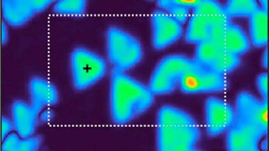
Seeing what was once invisible could unlock the next generation of 2D materials. Researchers have developed a novel sum-frequency microscope that makes atom-thin hexagonal boron nitride light up, enabling fast, high-contrast imaging of monolayers and their crystal orientation.
SFG microscopy image of boron nitride monolayer flakes.
(Source: FHI)
2D materials are crystalline substances consisting of only a single layer of atoms and have very unusual properties that arise from their extremely thin nature. Materials science has been aware of thin layered materials for over a hundred years, but it was only in 2004 that the first 2D layers — namely graphene — were successfully produced. Since then, new 2D materials have been continuously developed and novel applications have emerged. The thin layers are in demand for applications in many future technologies, from electronics and energy systems to optical components. Thus, these fascinating materials are the subject of extensive research.
The Challenge with Hexagonal Boron Nitride
Boron nitride (BN) — also known as “white graphene” — is a layered material composed of the elements boron (B) and nitrogen (N), and can exist in various forms, including hexagonal boron nitride (hBN). Similar to graphene, hBN has a hexagonal lattice structure and its 2D layers are widely used in various applications, such as quantum optics or infrared nanophotonics, or simply as a substrate or encapsulating material. For such applications a precise characterization of the h-BN layers is critical. However, aside from the pronounced mid-infrared resonance, as a monolayer, hBN is transparent across the entire near-IR and visible spectral range. Thus, it cannot be studied using conventional optical microscopes.
Gallery
This restriction has so far hindered its use in the development of new materials. For example, to identify possible distortions and grain boundaries in 2D layers, they must be accurately mapped. Moreover, researchers stack monolayers of 2D materials on top of each other to create “van der Waals structures” that can exhibit completely new and exciting properties. Ideally, this layering could be screened live under a microscope and the orientation of the individual layers visualized. The development of such capabilities for hBN are hence highly desired.
The Sum-Frequency Microscope
The research team at the Fritz Haber Institute overcame this challenge through their recently developed microscope that uses a trick in nonlinear optics to make the otherwise invisible material hBN visible. Their method, called “phase-resolved sum-frequency microscopy”, mixes two laser beams, one in the mid-infrared and one in the visible range, to generate a sum-frequency signal in the sample that is measured. By resonantly driving an hBN lattice vibration, the measured sum-frequency signal becomes very intense, making it not only possible to image large 100 × 100 μm2 sample areas in less than 1 s, but also even visualize the crystal orientation.
Thanks to their new microscope, the researchers revealed that the 2D layers of hBN that grow in triangular domains display nitrogen-terminated zigzag edges. Moreover, the observed high nonlinearity in the frequency range of the vibrational resonance highlights monolayer hBN as a promising material for frequency upconversion — from the infrared into the visible — in new optoelectronic devices.
Prospects of the New Experimental Method
The newly developed microscope offers clear advantages over other existing methods. First and foremost, it can make optically transparent materials visible in an optical microscope. The resulting images have much higher contrast than traditional AFM images, and the use of the vibrational resonance enhancement enables “live imaging” of hBN, including online information on its crystal orientation. These advanced capabilities make a controlled fabrication of layered van der Waals structures feasible in future applications. Finally, the authors also anticipate an extension of this new imaging tool as non-invasive and label-free method to study a wider range of stacked 2D-materials as well as their combinations with anisotropic molecular assemblies.
Date: 08.12.2025
Naturally, we always handle your personal data responsibly. Any personal data we receive from you is processed in accordance with applicable data protection legislation. For detailed information please see our privacy policy.
Consent to the use of data for promotional purposes
I hereby consent to Vogel Communications Group GmbH & Co. KG, Max-Planck-Str. 7-9, 97082 Würzburg including any affiliated companies according to §§ 15 et seq. AktG (hereafter: Vogel Communications Group) using my e-mail address to send editorial newsletters. A list of all affiliated companies can be found here
Newsletter content may include all products and services of any companies mentioned above, including for example specialist journals and books, events and fairs as well as event-related products and services, print and digital media offers and services such as additional (editorial) newsletters, raffles, lead campaigns, market research both online and offline, specialist webportals and e-learning offers. In case my personal telephone number has also been collected, it may be used for offers of aforementioned products, for services of the companies mentioned above, and market research purposes.
Additionally, my consent also includes the processing of my email address and telephone number for data matching for marketing purposes with select advertising partners such as LinkedIn, Google, and Meta. For this, Vogel Communications Group may transmit said data in hashed form to the advertising partners who then use said data to determine whether I am also a member of the mentioned advertising partner portals. Vogel Communications Group uses this feature for the purposes of re-targeting (up-selling, cross-selling, and customer loyalty), generating so-called look-alike audiences for acquisition of new customers, and as basis for exclusion for on-going advertising campaigns. Further information can be found in section “data matching for marketing purposes”.
In case I access protected data on Internet portals of Vogel Communications Group including any affiliated companies according to §§ 15 et seq. AktG, I need to provide further data in order to register for the access to such content. In return for this free access to editorial content, my data may be used in accordance with this consent for the purposes stated here. This does not apply to data matching for marketing purposes.
Right of revocation
I understand that I can revoke my consent at will. My revocation does not change the lawfulness of data processing that was conducted based on my consent leading up to my revocation. One option to declare my revocation is to use the contact form found at https://contact.vogel.de. In case I no longer wish to receive certain newsletters, I have subscribed to, I can also click on the unsubscribe link included at the end of a newsletter. Further information regarding my right of revocation and the implementation of it as well as the consequences of my revocation can be found in the data protection declaration, section editorial newsletter.
Original Article: Full Crystallographic Imaging of Hexagonal Boron Nitride Monolayers with Phonon-Enhanced Sum-Frequency Microscopy; Advanced Materials; DOI:10.1002/adma.202510124




:quality(80)/p7i.vogel.de/wcms/51/68/51687ac4cc19f2757c138498b877de57/0133167039v2.jpeg "CMFs are foams that consist of hollow spheres – made of materials such as stainless steel, nickel, or other metals and alloys – embedded in a metallic matrix. The resulting material is both lightweight and remarkably strong at absorbing compressive forces. (Source: Jie Sun/ NC State University)")
:quality(80)/p7i.vogel.de/wcms/cd/c0/cdc09efd1e5b3b8f83224e7729d66c10/0133105276v2.jpeg "From the data presented in this report, the authors show how TF3-MALS-RI is uniquely able to separate large polyacrylate molecules and provide precise molecular weight and Rg values. (Source: Postnova Analytics)")
:quality(80)/p7i.vogel.de/wcms/c6/f2/c6f2e2b4753a0d0cec682c03df4ed37c/0133088650v2.jpeg "PMBC vials for immunology and oncology research. (Source: Amsbio)")
:quality(80)/p7i.vogel.de/wcms/e0/72/e0728dc8dcadfc4d79a734e08cf6ced3/0133088641v2.jpeg "LM20 Microfluidizer and Cambridge CNT dispersion produced by the LM20 microfluidizer. (Source: Analytik)")
:quality(80)/p7i.vogel.de/wcms/86/01/86014d3d2a28cefc852f65c8d68317e4/0133104231v2.jpeg "Single-handed tube reading using a Handheld 2. (Source: Azenta Life Sciences)")
:quality(80)/p7i.vogel.de/wcms/0b/0f/0b0f8ed042dfc91f32582e10d54c2c7e/0133087444v2.jpeg "Offering advanced automation to increase your throughput, the Intellixcap provides secure sealing – eliminating the need for manual intervention, while preserving vital sample integrity. (Source: Azenta Life Sciences)")
:quality(80)/p7i.vogel.de/wcms/13/d3/13d35105f74a1c2e22b9c7a270e8e9b3/0132611155v2.jpeg "Circulating cell free DNA. (Source: Amsbio)")
:quality(80)/p7i.vogel.de/wcms/bc/ed/bced6850297a04dbea471a66cb6bb6fe/0132611405v2.jpeg "The latest addition to the range is a peristaltic tubing stop adapter that eliminates the need for fixed stoppers and allows custom cut lengths of peristaltic tubing to be installed on any pump head size. (Source: Biotech Fluidics )")
:quality(80)/p7i.vogel.de/wcms/a1/af/a1afbc7c8a067bbe94749ec680b4bafd/0133163762v2.jpeg "The study found in murkier water, fish took longer to move towards the food than those in clear water, but individuals in larger groups responded more quickly overall. (Source: Christos Ioannou)")
:quality(80)/p7i.vogel.de/wcms/32/80/3280aa3d44708962943c96fe2d466744/0133088560v2.jpeg "A bumble bee in flight at the University of Bristol Botanic Garden. (Source: Phil Savoie)")
:quality(80)/p7i.vogel.de/wcms/7b/e5/7be5c735140cbe28f3af0ec3d88274b9/0133045403v2.jpeg "After being buried in the ground for two months and broken down by soil organisms, a new pair of cotton underwear (left) shows clear signs of decomposition (right). (Source: Nicolas Zonvi)")
:quality(80)/p7i.vogel.de/wcms/c7/5e/c75e9b334a94b8b5c2a758f20ba080a8/0133039712v1.jpeg "Researchers have developed a microaerobic activated sludge process that enables ammonium to be recovered from fermentation industry wastewater instead of releasing nitrogen into the atmosphere. (Source: free licensed)")
:quality(80)/p7i.vogel.de/wcms/bf/d0/bfd087349a85956a7aefad57ac1204c7/0133241961v2.jpeg "The Thermo Scientific Suretect Beverage Spoilage Multiplex PCR Assay provides a fast, broad-range molecular solution for detecting key spoilage microorganisms that threaten beverage quality. (Source: © OlegDoroshin - stock.adobe.com)")
:quality(80)/p7i.vogel.de/wcms/d4/61/d461ce0bd5743897993c6475f69e7ad6/0133067478v2.jpeg "In Harris County, 50 % of households with children reported food insecurity, compared with 33 % of households without children. (Source: Rice University)")
:quality(80)/p7i.vogel.de/wcms/79/76/7976d17b980bedfe35acaa532d690046/0132713841v2.jpeg "Observed rice yield losses from 1°C warming are more than twice as high as model estimates due to underestimated heat stress. (Source: AdobeStock/ducvien)")
:quality(80)/p7i.vogel.de/wcms/28/b6/28b6114fc9915c5dadee94d5c89bd129/0132593216v2.jpeg "Eating foods that contain common preservative food additives may increase the risks of high blood pressure and cardiovascular disease. (Source: Unsplash)")
:quality(80)/p7i.vogel.de/wcms/7e/4b/7e4ba18a8518e5e8430ad07afbfd6ae4/0133321385v2.jpeg "New findings raise concerns about potential misdiagnosis, inappropriate treatment, and errors in psychiatric research. (Source: free licensed)")
:quality(80)/p7i.vogel.de/wcms/59/a1/59a133dc0a07d301f5f8921e01e257a3/0133241567v2.jpeg "A child experiencing a mental health crisis may arrive at any emergency department, and many are not prepared to care for children with acute mental health needs in the USA. (Source: Unsplash)")
:quality(80)/p7i.vogel.de/wcms/83/c8/83c862a4f3dbcafd0f150df5f4e96361/0133240374v2.jpeg "Out-of-hospital cardiac arrest is a time-critical emergency in which survival depends on early recognition, early cardiopulmonary resuscitation and early defibrillation. (Source: Unsplash)")
:quality(80)/p7i.vogel.de/wcms/6a/d8/6ad838b20e80c36d04940b5a6bc8ccf1/0133167025v2.jpeg "Dr Kassandra Giragosian and a chimp (Source: Kassandra Giragosian)")
:quality(80)/images.vogel.de/vogelonline/bdb/1710600/1710675/original.jpg "Discover how to set yourself up for success when performing balance-based density determination of solids such as jewelry and precious metals. (Mettler Toledo)")
:quality(80)/images.vogel.de/vogelonline/bdb/1682500/1682579/original.jpg "The new XPR Analytical balance redesigned to meet the needs of laboratory technicians of working fast and lean. (Mettler Toledo)")
:quality(80)/images.vogel.de/vogelonline/bdb/1677000/1677080/original.jpg "Enhance your weighing accuracy, comfort and productivity with the redesigned XPR Analytical balance. (Mettler Toledo)")
:fill(fff,0)/images.vogel.de/vogelonline/companyimg/107800/107832/65.jpg "logoDueperthal.jpg ()")
:fill(fff,0)/p7i.vogel.de/companies/69/b7/69b7f63f311d9/logo-bimos-tif--2-.jpeg "logo-bimos-tif--2- (https://www.bimos.com/de-de/)")
:quality(80)/p7i.vogel.de/wcms/43/9e/439ef146de269df7f413fdfd677650d0/0128496857v1.jpeg "SFG microscopy image of boron nitride monolayer flakes. (Source: FHI)")
:quality(80)/p7i.vogel.de/wcms/c2/2b/c22b6f47a7933cf16b76323d5067f76e/0128496854v1.jpeg "Schematic of the newly developed SFG microscope used to image the layers of boron nitride.(Source: FHI)")
:quality(80)/p7i.vogel.de/wcms/d7/f5/d7f5f8326fe75ef5487dedacb9790690/0126745071v1.jpeg "This image taken with a scanning electron microscope shows rhodium-coated platinum nanoparticles on a conductive substrate. The crystalline facets are clearly visible in the polyhedral shape of the nanoparticles. (Source: Arno Jeromin, Desy Nano Lab)")
:quality(80)/p7i.vogel.de/wcms/22/ba/22ba638495663a3adf106c2b30e84ff1/0132255309v1.jpeg "“The leaf sensor is more of an early warning system showing how the plant is responding in the moment, before visible signs appear,” said Nafize Hossain. (Source: Nafize Hossain)")
:quality(80)/p7i.vogel.de/wcms/bb/69/bb691bac4dbda490891d061ed43aa5e2/0127562694v1.jpeg "Particle vision analysis links exploration, experiments, and feedback, turning microscopic observations into new discoveries or optimized manufacturing conditions.
(Source: Guangyao Chen/ Fengqi You)")